
image selection: instructables
Currently, the amount of smart phones and computers that exist in the world is about 8 billion devices, (Google), which about equals the amount of people in the world in 2021, which is also 8 billion.
What is Photopolymer Film?
Selected Videos: understanding one of the most commonly used materials of the electronics industry making connections between the needs of circuit board manufacture and Fine Art printing in the intaglio manner. After thirty five years of use by artist printmakers photopolymer films are still only partly or poorly understood by most. Many think this is just some exotic and rare component of electronics manufacturing. Not so! We would recommend that anybody that is interested in the artistic use of these films for Intaglio Type printing, or for etching purposes, reflects on their use within the electronics industry, where dry photopolymer films are an essential and ubiquitous part for the manufacture of anything from iPhones to laptops, or indeed in the chips that are currently in short supply in car manufacture.
Millions of meters of light sensitive photopolymer film are produced and used every year. Currently, the amount of smart phones and computers that exist in the world is about 8 billion devices, (Google), which about equals the amount of people in the world in 2021, which is also 8 billion. The motherboards of these 8 billion devices will have undergone 16 billion laminations, exposures, and etching stages… using dry photopolymer films! (needed at the top and bottom of each board to etch wiring patterns). Below is a selection of YouTube videos on the topic of photopolymer films in electronic manufacture.
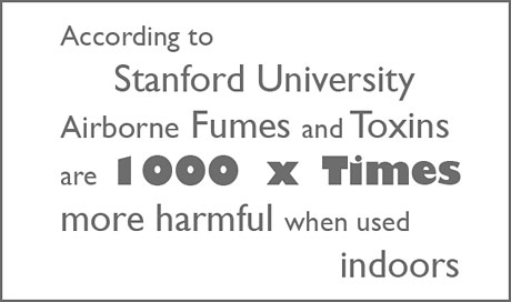
Dry Photopolymer Film Safety: Key brands of dry photopolymer films (such as DuPont / Hitachi / MacDermit) were over the years tested for occupational safety in the PCB / computing industry; and often found to be of low to intermediate safety concern, if handled correctly. Correct handling of these films involves avoiding skin contact with the film emulsion, and, crucially the use of good fresh air supply ventilation / extraction and respiratory protection during plate handling and processing. In industrial settings workers often wear N95 masks with organic carbon filter when handing film (see videos below).
Some cheaper products may be much more toxic! Look out for the composition of the film resin: resin based on acrylates has lower toxicity; resin based on epoxy or PVC/Nylon resins has high toxicity.
Watching these, PM sheds light on: how to peel off the soft layer of mylar using Scotch tape use of yellow light in industrial clean rooms use of heat lamination to adhere films to copper boards use of positive graphic wiring diagrams for UV exposure (as in silkscreen) development of exposed film/board in mild sodium carbonate solution etching, typically in ferric-chloride based baths film stripping in alkaline solutions how to make your own UV exposure unit from an old printer/scanner PCB process using photoresist dry 3lm Luis Acebal ‘Printed Circuit Board process using photoresist dry film. Proceso de creación de un circuito impreso usando película fotosensible.’
Inside a Huge PCB Factory – in China ‘Today we’re visiting JLCPCB one of the largest prototype PCB manufacturers in China. We’re getting an exclusive factory tour of one of their newest printed circuit board factories in Huizhou, just outside of Shenzhen, to see the PCB manufacturing production technology (full movie) ‘The “PCB production technology” film is created for electronic engineers and electronic designers. It demonstrates the multilayer PCB production process at Rezonit tech park.’
‘Today we’re visiting JLCPCB one of the largest prototype PCB manufacturers in China. We’re getting an exclusive factory tour of one of their newest printed circuit board factories in Huizhou, just outside of Shenzhen, to see the PCB manufacturing’
Full Site Map: a l l p a g e s / t o p i c s
© 2026